
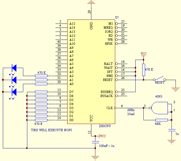
 Just think of how terrible it would be to wire up an entire system just to find out your microprocessor was a dud, and didn’t work properly. To avoid this we can build a test circuit to check if everything is operational in our microprocessor. This test circuit will place a logical ‘LOW’ on each bit of the data bus. This data byte made up of each individual “LOW” bits, ‘00000000’, corresponds to the instruction ‘NOP’.
‘NOP’ is the mnemonic for No-Operation, and will essentially do nothing for around four clock cycles, then increase the address bus by one address higher. Since we are not accessing any type of memory, and manually setting the data bus ‘LOW’ the Z80 microprocessor will indefinitely run the ‘NOP’ instruction until it reaches its highest addressable area ‘0xFFFF’.
If we attach some sort of monitor to the address bus we can watch the address increase as the microprocessor executes the ‘NOP’ instruction. If the address increases indefinitely we can be certain that the microprocessor is indeed in-tact. To literally watch the address bus we can attach LEDs to each of the address bit lines. To make it easier on ourselves we could put LEDs on the lower sub-set of the address bus to save time, and LEDs. I personally used a module off of tindie.com which can be found here. I highly recommend this module to anyone that wants a quick solution to replacing a bunch of LEDs and resistors. It is a small form factor, and a bit on the difficult side to solder for a novice, but manageable. It took me a little over an hour to build up four of these little modules, and I enjoyed building it. I got away with using a wedge tip on my soldering iron, and used tweezers and a magnifying lens.
Below is the realized schematic for the Z80 Test Circuit. I replicated the design seen here, Z80 Simple Circuit Schematic, with minor changes. A large change is that we are using the circuit we built in the last post to drive the clock pin of the Z80. Using the ‘POT’ we can then vary the frequency of operation between 5 and 20 Hertz, and the LEDs should ‘count’ in binary slower and faster based off of increased and decreased system frequency.

All files from this project can be downloaded from my GitHub Repository,

I built a circuit similar to your design with a few extra LEDS (A0-A9), and I noticed that LEDs from A7-A9 flash when they are enabled. After digging around on the interwebs a bit I discovered that it is part of the memory refresh circuitry that the z80 does when it tries to refresh dynamic memories. Just posting this in case anyone else comes across the issue and is scratching their head wondering why.
Cool circuit… back in the 80’s I worked for Heurikon corp on Z80 based multi bus SBC’s. I made up what I called a no-op processor by bending the data pins around to the top, and tying them low through an r-pac to the chip’s gnd pin. I put this in a 40 pin machine socket so it was easier to insert and pull from the board. Used this to trouble shoot many boards. At speed, 2 or 4 MHz, you could scope the address lines and see the varying duty cycle as you ran through the address lines. Found a lot of shorted lines and other chips stuck on the address bus. Built your ckt the other night just to play. Thanks!!